- 您现在的位置:买卖IC网 > Sheet目录1992 > CYW150OXC (Silicon Laboratories Inc)IC CLOCK 440BX AGP 56SSOP
CYW150
...................... Document #: 38-07177 Rev. *B Page 13 of 14
56
55
54
53
52
51
50
49
48
47
46
45
44
43
42
6
7
13
19
20
24
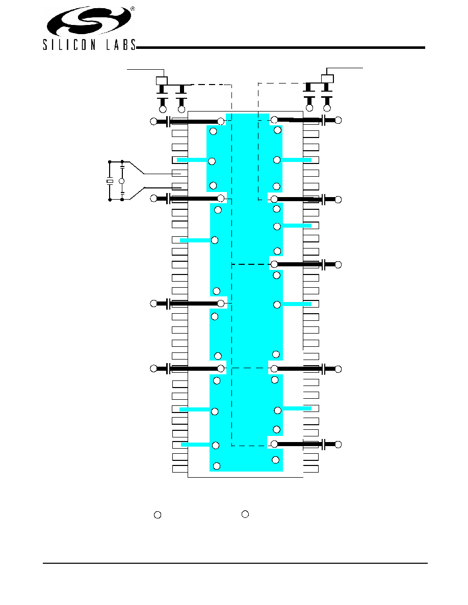
G = VIA to GND plane layer
V =VIA to respective supply plane layer
Note: Each supply plane or strip should have a ferrite bead and capacitors
G
+2.5V Supply
1
2
3
4
5
8
9
11
12
14
15
16
17
22
23
21
25
26
27
28
40
39
18
41
10
31
30
29
36
35
34
33
32
37
38
G
V
FB
+3.3V Supply
C4
Cermaic Caps C1 & C3 = 10 – 22 F C2 & C4 = 0.005
F
10 mF
FB
C1
C2
0.005 mf
FB = Dale ILB1206 - 300 (300
@ 100 MHz)
10 mF
0.005 mF
G
VDDQ2
VDDQ3
C3
G
V
All bypass caps = 0.1
F ceramic
G
V
G
V
G
V
G
V
G
V
G
V
G
V
CYW150
G
发布紧急采购,3分钟左右您将得到回复。
相关PDF资料
CYW173SXC
IC CLK GEN TAPE DRV 4CH 16SOIC
CYW305OXC
IC CLOCK W305 SOLANO 56SSOP
DAC5674IPHPG4
IC DAC 14BIT 400MSPS 48-HTQFP
DAC7621EBG4
IC SNGL 12BIT PARALLEL D/A 20SSO
DAC7801KPG4
IC DUAL 12BIT CMOS DAC 24-DIP
DAC8043AESZ
IC DAC 12BIT MULT SRL INP 8SOIC
DAC8043GP
IC DAC 12BIT MULTIPLY CMOS 8-DIP
DAC8221GP
IC DAC 12BIT DUAL W/BUFF 24-DIP
相关代理商/技术参数
CYW150OXCT
功能描述:时钟发生器及支持产品 Legacy-440BX AGP Refer to W150 DS RoHS:否 制造商:Silicon Labs 类型:Clock Generators 最大输入频率:14.318 MHz 最大输出频率:166 MHz 输出端数量:16 占空比 - 最大:55 % 工作电源电压:3.3 V 工作电源电流:1 mA 最大工作温度:+ 85 C 安装风格:SMD/SMT 封装 / 箱体:QFN-56
CYW152-12G
制造商:Rochester Electronics LLC 功能描述:- Bulk
CYW15G0101DXB
制造商:CYPRESS 制造商全称:Cypress Semiconductor 功能描述:Single-channel HOTLink II⑩ Transceiver
CYW15G0101DXB-BBC
功能描述:电信线路管理 IC Sngl Ch XCVR COM RoHS:否 制造商:STMicroelectronics 产品:PHY 接口类型:UART 电源电压-最大:18 V 电源电压-最小:8 V 电源电流:30 mA 最大工作温度:+ 85 C 最小工作温度:- 40 C 安装风格:SMD/SMT 封装 / 箱体:VFQFPN-48 封装:Tray
CYW15G0101DXB-BBI
功能描述:电信线路管理 IC Sngl Ch XCVR IND RoHS:否 制造商:STMicroelectronics 产品:PHY 接口类型:UART 电源电压-最大:18 V 电源电压-最小:8 V 电源电流:30 mA 最大工作温度:+ 85 C 最小工作温度:- 40 C 安装风格:SMD/SMT 封装 / 箱体:VFQFPN-48 封装:Tray
CYW15G0101DXB-BBXC
制造商:CYPRESS 制造商全称:Cypress Semiconductor 功能描述:Single-channel HOTLink II⑩ Transceiver
CYW15G0101DXB-BBXI
功能描述:电信线路管理 IC HOTLink II 1.5Gbps Single Channel RoHS:否 制造商:STMicroelectronics 产品:PHY 接口类型:UART 电源电压-最大:18 V 电源电压-最小:8 V 电源电流:30 mA 最大工作温度:+ 85 C 最小工作温度:- 40 C 安装风格:SMD/SMT 封装 / 箱体:VFQFPN-48 封装:Tray
CYW15G0201DXB
制造商:CYPRESS 制造商全称:Cypress Semiconductor 功能描述:Dual-channel HOTLink II⑩ Transceiver